Sony Vaio Revived: Power, The Second 80%

A bit ago, I’ve told you about how the Sony Vaio motherboard replacement started, and all the tricks I used to make it succeed on the first try. How do you plan out the board, what are good things to keep in mind while you’re sourcing parts, and how do you ensure you finish the design? This time, I want to tell you my insights about what it takes for your new board revision to stay on your desk until completion, whether it’s helping it not burn up, or making sure the bringup process is doable.
Uninterrupted, Granular Power
Power was generally comfortable to design, but I did have to keep some power budgets in mind. A good exercise for safeguarding your regulators is keeping a .txt file where you log consumers and their expected current consumption on each board power rail, making sure all of your power regulators, connectors, and tracks, can handle quite a bit more than that current. Guideline: increase current by 20%-50% when figuring out the specs for switching regulators and inductors, and, multiply by 10-20% when figuring out conversion losses going between downstream and upstream rails.
I did have a blunder in this department – not accounting for track current early on enough. I laid out the board using 0.5mm wide tracks for power – it looked spacious enough. Then, I put “0.5mm” into a track current calculator and saw a harrowing temperature increase for the currents I was expecting. At that point in routing, it took some time to shift tracks around to accomodate the trace width I actually needed, which is to say, I should’ve calculated it all way way earlier. Thankfully, things went well in the end.
 Apart from this, the power rails are a crucial aspect for bringup. How are you going to bringup your board? Which power rails need to be powered on so that the board can boot? Which signals do you need for every power rail, and what power rails do those signals depend on? What are the minimum required parts for the board to “boot”, and how quickly can you test every part before getting the next revision? My strategy was: I flash the EC with MicroPython, and hack at the code part by part I go. It worked surprisingly well for lowering the debugging entry level, and I will tell more about it later.
A lot of bringup preparations are done during design, though. You have to think about typical usecases, and think how your hardware is going to react to them. What kind of state will the board enter after you insert the battery, or apply power from an external charger? Will you need to find a charger after you swap the battery? Is battery hotswap possible? The best way to understand all of it is to look through fundamental blocks of the circuit, and ask questions about their behaviour.
The questions can be pretty simple. Is the EC always powered no matter the input source? Can you detect when the power sources are too low, or too high? What’s the default states of the EN pins of every switching regulator, and what are the default state of GPIOs that control your regulator EN pins? Are any of these pins connected to GPIOs that might oscillate during your MCU’s boot? Is the input DC-DC enabled by default? What about the battery charger?
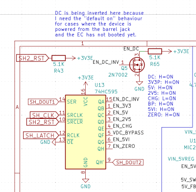
In the end, I went through all the switching regulator datasheets, taking note of the EN pins. Closer to the end, I’ve noticed that I’d need to invert the EN pin of the input DC-DC with help of a FET if I wanted that regulator to be powered on by default – otherwise, I’d get a chicken-and-egg problem if I were to try and power the board through its charger with missing or fully discharged battery. The FET barely fit on the board, but I massaged the tracks until it did.
Double-Sided Assembly
Here’s tips for bringup – you want to make sure you can access your EC at all times. In my case, I decided to mux the EC RP2040’s USB onto the external port, allowing for a “debug mode” with a USB A-A cable – a cool feature, but I have definitely regretted restricting myself with it. Essentially, I locked myself into USB plug-unplug cycle during the early development, and it was hell to solve problems as a result. My advice is – plan for an extra USB-C connector or just USB testpoints on your board, so you can have a permanent unshakeable USB/SWD/UART/etc. link during the period while you’re not quite sure how well your board works. In the end, I had to tombstone the two 0402 D+/D- resistors of the RP2040 EC and pull an external “debug” USB-C connector on three magnet wires – a finicky endeavour, worth avoiding if you can.
Other than that hurdle, the bringup has been seamless, in no small part because I used the MicroPython REPL to probe through the board as I enabled parts of it. The REPL flow let me enable/disable power rails and query GPIOs dynamically during early bringup, mocking up code on the fly and immediately testing it on my hardware, and dynamically debug features like onboard shift registers, or buttons and LEDs on the Vaio’s case, wrapping them into code and putting them into the main.py file – the EC firmware grew larger and larger as I experimented. There’s something special about having a list of power rails at your fingertips, switching them off one by one, quickly tying program states into switches/buttons/LEDs as needed – it was a joy of a bringup experience.
How do you assemble such a double-sided board – really, how do you even stencil it? I planned for stenciling it from the very beginning, and, I distributed the components in a way that one side had way less components than the other – including more intricate components, like multi-pin ICs. One thing that’s really helped, is using the JLCPCB stencil shipping cardboard to make a jig for the board with cutouts in it, letting me stencil the less-populated side once the more-populated side already had components soldered onto it. In a different life, I used to lasercut frames for this kind of endeavour – KiCad SVG export should be all you need.
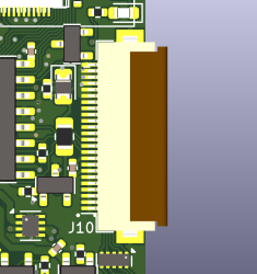
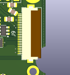
The more-populated side got assembled using one of those tiny $20 hotplate, in the comfort of my home – I’d hot air it, but my hot air gun fell and broke. I did have to borrow a hot air gun for assembling the second side, though – and assemble it very carefully. The main problem was the plastic connector on the less-populated side – I had to hot air it from the bottom, through the RP2040 EC and its supporting circuitry.
Learning, Achievements, Expansion
I’ve had some fun failure modes happen on this board. One, the failing 5V boost with subpar layout, which I’ve already described in the switching regulator patch board article a couple months ago. Fun fact – it’s also verified a RPi SD card corruption theory of mine, confirming that noise on the input power rail easily propagates into the 3.3V rail powering the SD card, and results in SD card corruption; if you’re getting SD card corruption issues, make sure to check the DC-DCs involved in your project!
Another one was specifically the output pin of the 3.3V EC regulator not getting soldered properly – somehow, it had a cold solder joint, and the EC was getting powered with around 1.23V, again, somehow; it might’ve been due to my incessant multimeter probing, in hindsight. I’m glad that this was the cold solder joint I had to figure out – as far as cold solder joints go, this one was seriously easy to debug, since just moving the probe between the 3.3V reg leg and an EC power capacitor was enough to find the spot the voltage drop happened.
Again, any burnt components on such an assembled board get expensive – not just monetarily, it’s also that you don’t want to repeat the assembly effort. So, keep all metal and solder away during bringup, check all the connectors for accidental solder blobs many times over, and be very careful to. Tempted to hotplug internal connectors? Don’t do it unless you’ve designed them to hotplug, or if the original manufacturer has – there’s always pinout and connector considerations you have to mind. This goes doubly for high-current and high-voltage connectors.


Expansion slots are wonderful if you can afford them – there’s usually leftover GPIOs and some power rail capacity that you might want to later tap, and in my case, there’s also heaps of free space inside of the laptop. I managed to fit two FFC sockets on this particular board, which have plenty of high-current power rails and GPIOs – my plan, personally, is to make a board that takes SATA or NVMe SSDs, and maybe even has expansions like GPS or extra WiFi – the case internals are spacious enough for all of those.
Looking to put a new powerful motherboard into an old lovely chassis? Chances are, you can certainly do it – even if it takes time, trial-and-error, and help from some friends or internet strangers. I hope this project walkthrough can help you lots along the way, especially in being comfortable to take the first steps! Got a project stuck on the mental shelf? Get on with it – you will learn new cool things, and find new tricks to improvise. Me, I’m getting a friendly device to carry in my pocket, and that alone is a wonderful experience.
from Blog – Hackaday https://ift.tt/njQikHd
Comments
Post a Comment