Your Own Open Source ASIC: SkyWater-PDF Plans First 130 nm Wafer in 2020
You might have caught Maya Posch’s article about the first open-source ASIC tools from Google and SkyWater Technology. It envisions increased access to make custom chips — Application Specific Integrated Circuits — designed using open-source tools, and made real through existing chip fabrication facilities. My first thought? How much does it cost to tape out? That is, how do I take the design on my screen and get actual parts in my hands? I asked Google’s Tim Ansel to explain some more about the project’s goals and how I was going to get my parts.
The goals are pretty straightforward. Tim and his collaborators would like to see hardware open up in the same way software has. The model where teams of people build on each other’s work either in direct collaboration or indirectly has led to many very powerful pieces of software. Tim’s had some success getting people interested in FPGA development and helped produce open tools for doing so. Custom ASICs are the next logical step.
Who Needs Open Source ASICs?
Of course, FPGAs and ASICs aren’t the answer to every problem. We can’t help but notice that some examples you see — including ours — are sometimes better for learning than actually practical. For example, the classic sample for learning about state machines on an FPGA is a traffic light. Why not? Everyone sort of understands what it is supposed to do, it has clear state logic, and you can make it as simple as you like or quite complex if it senses vehicles and pedestrian crosswalk buttons or changes based on schedules.
However, if you were really building a traffic light, it wouldn’t make a lot of sense to do it in an FPGA. Even the simplest microcontroller would be up to the task and would be cheaper both to buy and in terms of engineering costs by a wide margin.
 ASICs occupy a similar niche, but with a little bit of a difference. On the plus side, they should be denser, faster, and less power hungry than a similar FPGA. That makes sense because the ASIC is sort of an FPGA where the interconnections are made with dedicated metal lines instead of being generally configurable. You can also put down exactly the circuits you want — or, at least, choose from a variety of cells instead of having to use whatever the FPGA’s architect decided you need. You can even include analog cells alongside digital circuitry.
On the negative side, ASICs are not for the sloppy. Historically, taping out an ASIC has been very expensive. So you have a run of parts but — oops — you forgot that counter needs to reset to a non-zero number. In an FPGA, that’s a minor annoyance; you simply change the configuration — especially now that one time programmable FPGAs are rare outside of certain applications. Even if you have to trash an FPGA and program another one, they are generally not very expensive unless they are radiation hardened or very large devices.
If you make that mistake on an ASIC, you are in big trouble. You can’t change anything on the parts you have. You have to have a new batch built with new upfront costs. In the commercial world, that kind of mistake can be career-ending.
Tim makes it clear that his target audience isn’t the professional building custom ASICs, though. It is us. The hackers and tinkerers that want to create custom ICs. There may be some student market, too, although schools often have deals to make that feasible already.
Tim does point out, though, that a lot of those school deals are bound up with nondisclosure agreements the students have to sign, so it’s possible that open tools will spur new published research which would be a good thing. Still, I get the sense they think most of the interest will be from our community.
Notable about this process is that the 130 nm process being used isn’t cutting edge technology. The Skywater Technologies fab was built by Cypress Semiconductor in 1991 in Bloomington, Minnesota. Tim says professional designers have moved so far from these large geometries that our designers may have to rediscover some lost knowledge along the way to get the most from an IC made on the larger processes now. But the existing infrastructure is a big part of what makes this project more affordable.
So How Do You Get Them?
Tim had a lot to say about cell libraries that are eminent and how each one was tuned for a different purpose (e.g., high density or low power or high speed). However, we wanted to know how we’d get actual parts. Apparently, some of the details or still being worked out.
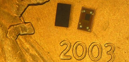
In November, they plan to order a multiproject wafer with 40 slots. They don’t know yet if they will have to beg and plead to get 40 designs or if they will have to winnow the select down from all possible candidates. If you are one of the 40, you’ll get about 10mm square to play with and wind up with somewhere around 100 to 300 chips in chip-scale packaging (CSP). You can see a typical CSP sitting on a US penny in the accompanying photo.
There are a few stipulations. You’ll submit your design on GitHub (or some similar public repository), so your design is going to be open source. That means even if you aren’t one of the 40, you’ve just put your chip out for the world to see. The foundry will automatically check your design to meet certain technical criteria. At this early point there doesn’t seem to be a firm plan on how they will select designs for inclusion in the first run. Presumably, if there are a lot of entrants and things work well, there will be more wafers in 2021.
There are still a lot of unanswered questions. Can you pay to get your own tape out? If so, do you still have to be open source? What if you have some made and then want more? How much does that cost? This is very early and we do we not yet know the answers to these questions, but details will come together over time.
The Key
Like I said earlier, ASICs aren’t for everyone and they certainly aren’t for people who test and debug as they go. Verification is essential for a successful ASIC project. That means a lot of this will hinge on the simulation tools available and the quality of the models available. Spending a lot of time and money getting ICs that won’t work at the speeds you need, consume more power than you expected, or simply don’t work is heartbreaking.
Many times an FPGA can be used to validate some or all of your design before trying to go to an ASIC. When that works, it works well. However, because of the differences between the two technologies, it isn’t as simple as thinking of an ASIC as a fixed FPGA. You have the same problems you might have going from a hand-wired circuit to a PCB. Logically they are the same. But we all know you can have problems with that transition because of the different characteristics. It is the same problem here. How do you test your analog cells? Will the clock distribute the same? And ASICs have speed or power requirements which are difficult to mimic in a validation stage.
Tim Ansel gave an online talk today officially announcing the project. Take a look for more details on the process node itself and the tools used to design for it:
So will you try to design your own IC? I’ve been involved in ASIC development before, but I still might be interested in doing my own personal project just to be able to do all the steps. Let us know what IC you want to design — or see someone else design — in the comments.
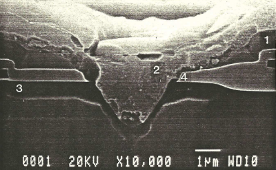
Header image: Peellden/ CC BY-SA 3.0
from Blog – Hackaday https://ift.tt/3ia9Exg


Comments
Post a Comment